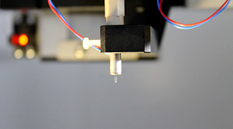
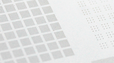
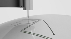
Hybrid perovskite CH3NH3PbI3 has attracted extensive research interests in optoelectronic devices in recent years. Herein, inkjet printing method has been employed to deposit a perovskite CH3NH3PbI3 layer. By choosing the proper solvent and controlling the crystal growth rate, hybrid perovskite CH3NH3PbI3 nanowires, microwires, network and islands were synthesized by means of inkjet printing. Electrode-gap-electrode lateral-structured photodetectors were fabricated with these different crystals, of which hybrid perovskite microwires-based photodetector would balance the uniformity and low defects to obtain switching ratio of 16000%, responsivity of 1.2 A/W and normalized detectivity of 2.39×10¹² Jones at the light power density of 0.1 mW/cm2. Furthermore, the hybrid perovskite microwires-based photodetector arrays were fabricated and applied in imaging sensor, from which the clear mapping of the light source signal was successfully obtained. This work paves a new way for the realization of low-cost, solution-processed and high-performance hybrid perovskite-based photodetector arrays.
Yang L , Li F , Veeramalai C P , et al. Inkjet-printed Photodetector Arrays Based on Hybrid Perovskite CH3NH3PbI3 Microwires[J]. Acs Applied Materials & Interfaces, 2017, 9(13):11662.